Volpiano (Italy)
September 18, 2025
The Evolving Landscape of Silicon Photonics Testing
Silicon Photonics (SiPh) stands at the forefront of a technological revolution, merging the power of electronics with the speed of light. Its ability to transmit vast amounts of data using light, at speeds far exceeding conventional electrical interconnects, makes it an ideal solution for mitigating the “data bottleneck” in a vast array of applications, from high-speed data centers and artificial intelligence accelerators to 5G networks, LiDAR for autonomous vehicles, and even quantum computing.
By integrating optical components onto silicon chips using standard CMOS manufacturing processes, SiPh promises to unlock unprecedented performance and energy efficiency. However, realizing the full potential of this groundbreaking technology hinges on overcoming significant hurdles in its testing methodology.
Unlike traditional electronic circuits, SiPh devices demand a sophisticated approach that addresses both electrical and optical characteristics, presenting a unique set of challenges that redefine the very nature of semiconductor testing.
Production testing in the silicon photonics era
The relentless demand for higher bandwidth, lower latency, and reduced power consumption in modern computing and communication infrastructures has propelled Silicon Photonics into the spotlight. As this technology moves from research labs to high-volume manufacturing, the importance of robust and efficient testing becomes paramount. Comprehensive testing is not merely about validating performance; it is crucial for early defect detection, yield optimization, cost reduction, and ultimately, ensuring the reliability and longevity of the devices in real-world applications.
The need for a hybrid test: Electrical meets Optical in SiPh testing
The most fundamental challenge in SiPh testing stems from its hybrid nature. SiPh chips integrate both electrical and optical functionalities on the same substrate. This necessitates a test solution capable of simultaneously stimulating and measuring both electrical signals (e.g., voltage, current, RF parameters) and optical signals (e.g., light power, wavelength, polarization, modulation). Legacy test equipment, typically designed for purely electrical or purely optical components, falls short in providing the integrated capabilities required for efficient SiPh verification. This gap necessitates the development of test setups that can seamlessly bridge these two distinct physical domains.
Nano-meter level precision alignment: A must for SiPh testing
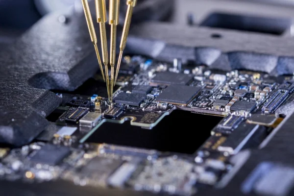
Perhaps the most critical and demanding aspect of SiPh testing is the requirement for ultra-high precision optical alignment. To effectively couple light into and out of the silicon chip, optical fibers must be positioned with extraordinary accuracy relative to sub-micron features on the silicon surface, such as grating couplers or waveguides. These optical interfaces, or “ports,” can have dimensions as small as 100-120 nanometers in diameter. Even a slight misalignment—deviations on the order of tens or hundreds of nanometers—can lead to significant light loss, compromising the integrity of the test signal and rendering the measurement unreliable.
Achieving this nanometer-level precision is a complex undertaking. Traditional manual or semi-automated alignment processes, while suitable for low-volume engineering characterization, become bottlenecks in high-volume production environments. The process involves active alignment techniques, where light is continuously coupled into the device under test (DUT), and the optical fiber’s position is iteratively adjusted in multiple translational axes (XYZ) and angular axes (roll, pitch and yaw) until the maximum light intensity is detected at the output. This peak search mechanism is computationally intensive and demands highly stable, repeatable, and fast motion control systems. The ability to quickly and accurately find this optimal coupling point is a key differentiator for production-worthy SiPh test solutions.
Furthermore, SiPh devices can employ different light coupling methods. Surface coupling, often utilizing grating couplers, allows for vertical access to the optical circuit, which is generally preferred for wafer-level testing due to its flexibility in interface positions. Edge coupling, where light is introduced from the side of the chip, is often used for final packaged devices. A comprehensive test solution must be adaptable to both paradigms, understanding the varying alignment tolerances and test methodologies associated with each.
The demands of Silicon Photonics Wafer-Level and Panel-Level Testing
Testing SiPh devices at the wafer level is crucial for manufacturing efficiency and cost optimization. By identifying and discarding defective dies early in the fabrication process, manufacturers can avoid the significant expenses associated with packaging faulty chips.
Similarly, as Panel-Level Packaging (PLP) emerges as a viable alternative to traditional wafer-level processing for certain applications, the ability to test devices efficiently at this larger panel scale also becomes paramount. Whether at the wafer or panel level, efficient in-line testing introduces additional layers of complexity:
- High throughput requirements: Production environments demand rapid test cycles and high volumes. Traditional optical test setups, often designed for characterization, are too slow for mass production, while conventional wafer probers do not possess the high-precision alignment mechanisms required. New-generation mixed signal testers and probers must integrate high-speed alignment and parallel testing capabilities to meet these throughput targets, operating 24/7 with minimal downtime.
- Maintaining precision across the wafer: Ensuring consistent and repeatable nanometer-level alignment across thousands of dies on a single wafer requires exceptional mechanical stability, advanced vision systems, and sophisticated algorithms for chip registration and precise movement between test sites.
- Environmental Control: Some SiPh applications, particularly co-packaged optics (CPO), may require active thermal management during testing to simulate operational conditions and ensure performance over temperature variations.
SiPh architectural diversity: Single-side or double-side access
SiPh devices can be designed with various electrical and optical layouts. Some chips may have all electrical and optical connections on a single side, while others might separate them on opposing sides of the wafer. Test equipment must be flexible enough to accommodate these differing architectures without requiring extensive retooling or complex manual reconfigurations.
Beyond the physical challenges: Data management in SiPh testing
Managing the sheer volume and complexity of data generated during SiPh testing presents another hurdle. Test results involve a combination of electrical parameters (e.g., S-parameters, eye diagrams, bit error rates) and optical parameters (e.g., insertion loss, return loss, spectral response, polarization-dependent loss). Powerful data acquisition, analysis, and visualization software are essential for correlating these diverse measurements, identifying performance trends, pinpointing defects, and providing actionable insights for process improvement and yield enhancement.
Cost of test (COT) and scalability
Ultimately, the widespread adoption of Silicon Photonics hinges on its economic viability. High test costs can negate the manufacturing advantages offered by CMOS compatibility. The time-consuming nature of optical alignment, coupled with the specialized equipment required, historically contributed to a high cost of test. Reducing this cost is a key requirement for SiPh to scale to high-volume manufacturing. This involves optimizing test routines, minimizing test time through automation and parallelization, and developing integrated solutions that reduce capital expenditure and operational overhead. Test equipment must be robust and reliable for continuous operation, reducing maintenance and preventing costly downtime.
SPEA’s integrated approach for SiPh testing
Recognizing these multifaceted challenges, SPEA has pioneered an integrated approach to Silicon Photonics probing and mixed signal testing, designed to provide comprehensive, high-throughput, and cost-effective solutions for both wafer and packaged device testing. Building upon its extensive heritage in automated test equipment, SPEA’s innovative platforms address the critical requirements of this new technological frontier.
At the core of SPEA’s wafer-level SiPh test offering is a new automated test machine, which leverages and enhances the robust architecture of the proven TH2000 platform. This system represents a significant advancement by seamlessly merging electrical and optical probing capabilities and complete test instrumentation into a single, highly integrated solution.
A key innovation lies in its deployment of mobile mini-probe cards. These advanced cards are meticulously engineered to integrate both conventional electrical contact probes and precision optical fibers. This concurrent presence of electrical and optical interfaces on the same movable unit eliminates the need for separate probing stations or complex reconfigurations, streamlining the test process and significantly reducing overall test time.
The equipment addresses the paramount challenge of optical alignment with an advanced, intelligent alignment system. Recognizing that optical coupling success is contingent upon nanometer-scale precision, the system employs sophisticated mechanisms to actively align the optical fibers to the minuscule (100-120 nm diameter) features on the silicon. This is achieved through a dynamic process that precisely measures and optimizes the light intensity passing through the device at multiple critical points. By continuously seeking the peak light transmission, the system ensures optimal optical coupling, guaranteeing that the test data collected is accurate, reliable, and representative of the device’s true performance. This intelligent peak-finding and alignment mechanism is fundamental to overcoming the “nanometer gauntlet” in high-volume production, while allowing a considerable time saving compared to camera-based alignment systems.
Furthermore, the tester is engineered for unparalleled versatility and adaptability. It is designed to accommodate the diverse range of SiPh manufacturing technologies and device architectures emerging in the market. Whether electrical and optical interfaces are situated on the same side of the wafer or on opposing sides, the system can configure itself to perform comprehensive testing, ensuring a future-proof solution for evolving SiPh designs.
Beyond wafer-level testing, SPEA’s commitment to a holistic solution extends to complete test cell integration for packaged devices. Understanding that testing does not conclude at the wafer stage, SPEA offers integrated solutions that combine its high-performance test units with advanced pick-and-place test handlers. These comprehensive test cells facilitate seamless movement of packaged SiPh devices from handling to test, ensuring efficient throughput and minimizing manual intervention. This full-spectrum capability means that SPEA can provide a complete ecosystem for SiPh testing, from the initial wafer fabrication stages to the final packaged components, ensuring consistent quality control throughout the entire production flow.
The transformative advantages of SPEA’s integrated solutions
SPEA’s integrated test philosophy delivers several transformative advantages for SiPh manufacturers:
- Ready-to-use equipment for device characterization: SPEA’s equipment enables a comprehensive and correlated understanding of device performance, assessing optical and electrical characteristics with a single machine. For lab use, the tester can be equipped with universal, single-site probe cards, that eliminate the need for device-specific fixturing. This integrated data collection facilitates quick root cause analysis of failures and accelerates design validation and process optimization, without the costs and time of developing specific probe cards.
- All-in-one equipment for production testing: By performing both electrical and optical probing and complete mixed signal test on a single, unified platform, SPEA’s equipment allows for a single-insertion test assessing all device’s characteristics.
- Throughput and efficiency: The combination of automated, nanometer-precision alignment, the novel mobile mini-probe card concept, and high-speed test routines drastically reduces test time per device. This is crucial for meeting the escalating demands of high-volume SiPh manufacturing, ensuring that test remains an enabler, not a bottleneck, in the production pipeline.
- Cost of test (COT) reduction: Early defect detection at the wafer level prevents the costly packaging of faulty dies. Optimized test sequences, streamlined workflows, and a reduction in re-testing contribute directly to a lower overall cost of test. Furthermore, the robust design of SPEA’s systems ensures high reliability and uptime, minimizing operational expenses and maximizing equipment utilization.
- Scalability for mass production: SPEA’s testers automation, precision, and high-throughput capabilities make them ideally suited for scaling SiPh production from initial ramp-up to full-scale mass manufacturing.
- Future-proof flexibility: The adaptable architecture of SPEA’s test platforms ensures they can readily accommodate new SiPh technologies, evolving device complexities, and various coupling methods, safeguarding investments and providing a long-term testing solution.
- Simplified test infrastructure: Partnering with a single manufacturer capable of providing integrated electrical and optical test solutions across both wafer and package levels simplifies the entire test infrastructure, reducing complexity in terms of integration, maintenance, and support.
Conclusion
Silicon Photonics is undeniably a cornerstone of future high-performance computing and communication. Its ability to revolutionize data transfer and processing is contingent upon robust, efficient, and cost-effective testing. The peculiar hybrid nature of SiPh devices, coupled with the stringent demands for nanometer-precision optical alignment, high throughput, and adaptability to diverse architectures, presents unique challenges for production test setups.
SPEA’s integrated approach to Silicon Photonics testing stands as a compelling answer to these challenges. By developing advanced automated equipment that seamlessly combine electrical and optical probing at the wafer level with comprehensive mixed signal test capabilities, and by extending these capabilities into comprehensive test cells for packaged devices, SPEA empowers manufacturers to unlock the full potential of SiPh. This commitment to innovation ensures that the benefits of light-speed data transmission and capacity can be reliably and economically realized, paving the way for the next generation of technological breakthroughs.