Volpiano (Italy)
October 23, 2025
Silicon Efficiency: Innovative Die Layouts & Wafer Test
Introduction: The Quest for Silicon Efficiency in Semiconductor Manufacturing
As semiconductor manufacturers strive to increase productivity while minimizing costs, optimizing the use of silicon real estate on a wafer has become a key focus area.
The push toward smaller, more powerful electronic devices, coupled with the need to reduce form factors, has led to innovations in wafer layout design. Innovative die geometries and multi-project wafers (MPWs) have become powerful strategies for maximizing wafer area utilization. However, these advancements bring unique challenges to the wafer testing process, particularly when using traditional probe technologies.
In this article, we will delve into how innovative die layouts, including non-square dies and MPWs, enhance silicon efficiency and influence the testing process. Additionally, we’ll explore how advanced testing methodologies – like flying probe technology – are enabling comprehensive testing for these complex designs, driving further improvements in yield and production efficiency.
1. Optimizing Silicon Usage with Non-Square Die Geometries
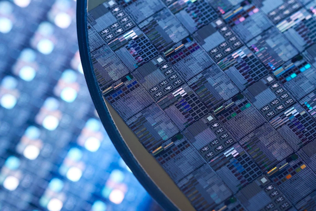
Traditional semiconductor dies are typically designed in square or rectangular shapes. This geometric regularity makes for easier placement on the wafer and simplifies the testing process with standardized probing solutions. However, square dies are often not the most efficient use of circular wafer space. The unoptimized spaces between dies, commonly called “kerf loss” or “scribe line,” reduce the overall yield of usable dies per wafer, ultimately increasing production costs.
Non-Square Die Geometries as a Solution
To address this, designers are turning to non-square die geometries, including triangular, parallelogram, and trapezoidal shapes. Inspired by tessellation principles used in art and mathematics, these shapes can be arranged to cover a larger portion of the wafer area, significantly minimizing unused space. For instance, hexagonal or triangular dies allow for denser arrangements and provide more freedom in pad placement and I/O integration, a feature particularly advantageous for high-connectivity devices.
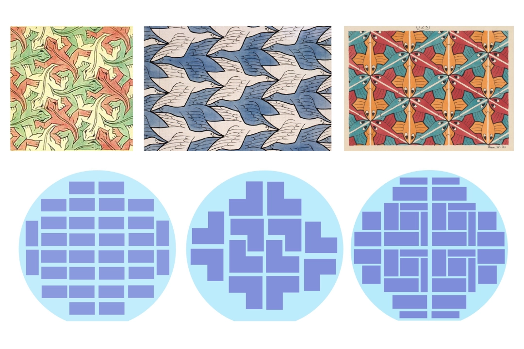
Figure 1 – Tesselletion principle – used in arts and mathematics – inspires unconventional wafer geometries, to increase space efficiency
Challenges and Advantages of Non-Square Dies
While these shapes maximize wafer utilization, they pose challenges for the wafer testing process. Traditional probe cards are designed to handle square dies aligned in uniform rows and columns. When dies deviate from this shape or orientation, conventional probe setups can struggle with alignment and coverage, leading to inefficiencies or incomplete testing.
However, the advantages of non-square dies outweigh these challenges, especially for high-performance applications where space and I/O count are at a premium. These die layouts support innovative architectures and increase the potential for additional functionality, particularly important as devices continue to miniaturize and integrate multi-functional capabilities.
2. Multi-Project Wafers (MPWs): Economies of Scale on a Single Wafer
The Concept and Benefits of MPWs
Multi-Project Wafers (MPWs) allow multiple chip designs, often from different projects or companies, to coexist on a single wafer. This approach is particularly beneficial for low- and medium-volume production runs, where the cost of dedicated wafers would otherwise be prohibitive. By integrating several projects on one wafer, manufacturers can share the costs of wafer fabrication, making advanced semiconductor technology accessible for smaller-scale applications or R&D prototyping.
Testing Challenges with MPWs
While MPWs bring economic advantages, they complicate wafer testing significantly. Each chip design on an MPW may vary in terms of shape, I/O layout, and test requirements. Traditional probe card designs, which assume uniform die layouts, struggle with these varied geometries and may require multiple probe card reconfigurations for a single wafer—a costly and time-intensive process. Furthermore, some MPWs include dies with orientations that mirror or rotate relative to one another, further complicating alignment and testing logistics.
Innovative probing solutions, based on the principle of flying probe card technology, can adapt to the irregularities of MPWs without the need for custom probe cards for each design. This flexibility enables comprehensive testing with fewer interruptions, reducing time and costs while ensuring that each project on the wafer meets quality and performance standards.
3. The Role of Advanced Probing Technology in Testing Complex Die Layouts
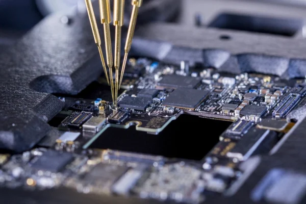
The complexities introduced by innovative die layouts require probing solutions that offer flexibility beyond conventional fixed probe cards. This is where flying probe card technology becomes essential. By leveraging independently mobile probe cards that can adapt to different die shapes, layouts, and orientations, this technology provides the adaptability needed to test unconventional die layouts with precision.
How Flying Probe Card Technology Addresses Non-Standard Geometries
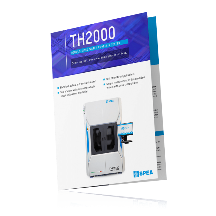
Flying probe cards are particularly useful for non-square dies and MPWs because they can navigate to individual die positions and orientations on the wafer surface, regardless of shape. Equipped with up to eight independently controlled probes, the prober can test various die configurations without retooling, even allowing for simultaneous testing on both sides of the wafer for double-sided dies. This ability to move freely across the wafer also enables quick adjustments for different die arrangements, drastically improving testing throughput for complex wafer layouts.
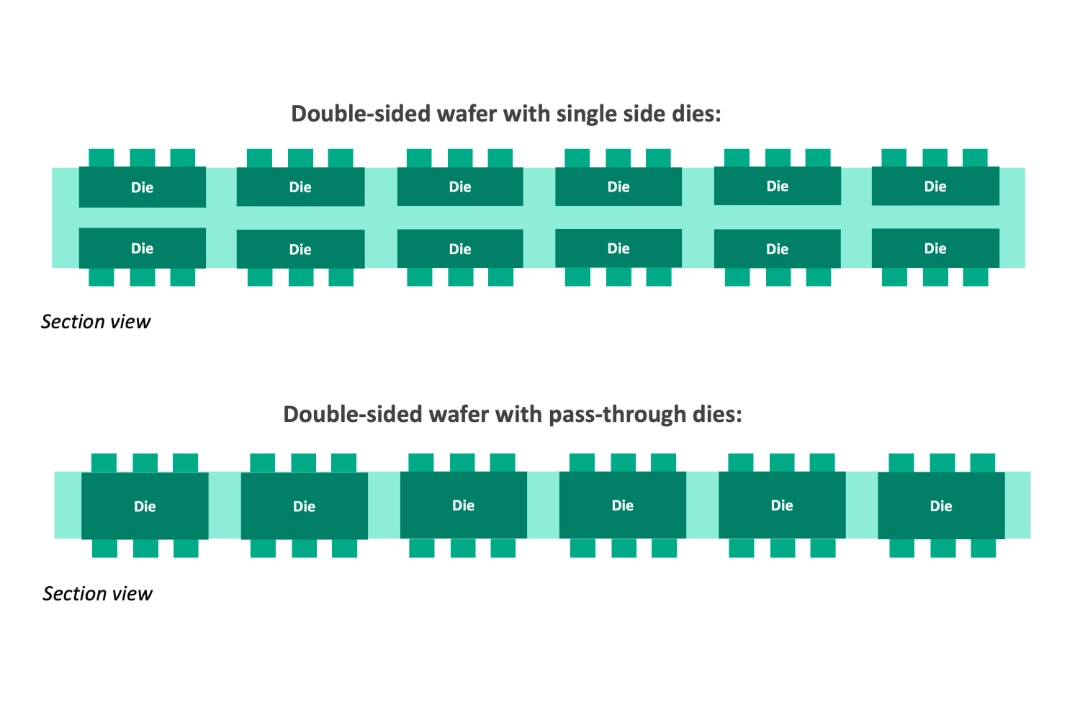
Figure 2. Principle of double-sided wafer design: the dies can be located on both sides of the wafer, or each die structure requires being processed on both sides.
Cost Efficiency and Time Savings
Traditional wafer testing methods require custom probe card designs that can be costly and time-consuming to manufacture, particularly for MPWs with varied die layouts. Flying probe cards eliminate these needs, offering a reusable and adaptable solution that reduces setup times and tooling expenses. For manufacturers, this flexibility translates to significant cost savings, especially when testing small runs or specialized designs that would otherwise require extensive reconfiguration.
4. Double-Sided Wafers and Multi-Layer Structures: Vertical Optimization and Its Testing Needs
In response to the need for greater functionality and miniaturization, semiconductor designs are increasingly adopting 3D integration techniques. Multi-layer structures with dies on both sides of the wafer offer new possibilities for densely packed, high-performance chips that minimize interconnect lengths and enhance data transfer speeds. Double-sided wafer designs, for example, enable top-bottom pad access, allowing for intricate designs with multiple layers and interconnections.
Challenges of Testing Double-Sided and Multi-Layer Wafers
Testing double-sided wafers presents a unique challenge for traditional prober setups, which typically dock only one side of the wafer at a time. Multi-layer wafers compound these difficulties, as each layer may need separate testing, and some layers might not be accessible without flipping or repositioning the wafer.
A double-sided prober offers a solution to these issues. With probes positioned on both the top and bottom sides, flying probe cards can access all layers and sides of the wafer simultaneously. This is essential for pass-through die testing and the verification of inter-layer connections, providing manufacturers with the capability to verify complex 3D structures comprehensively.
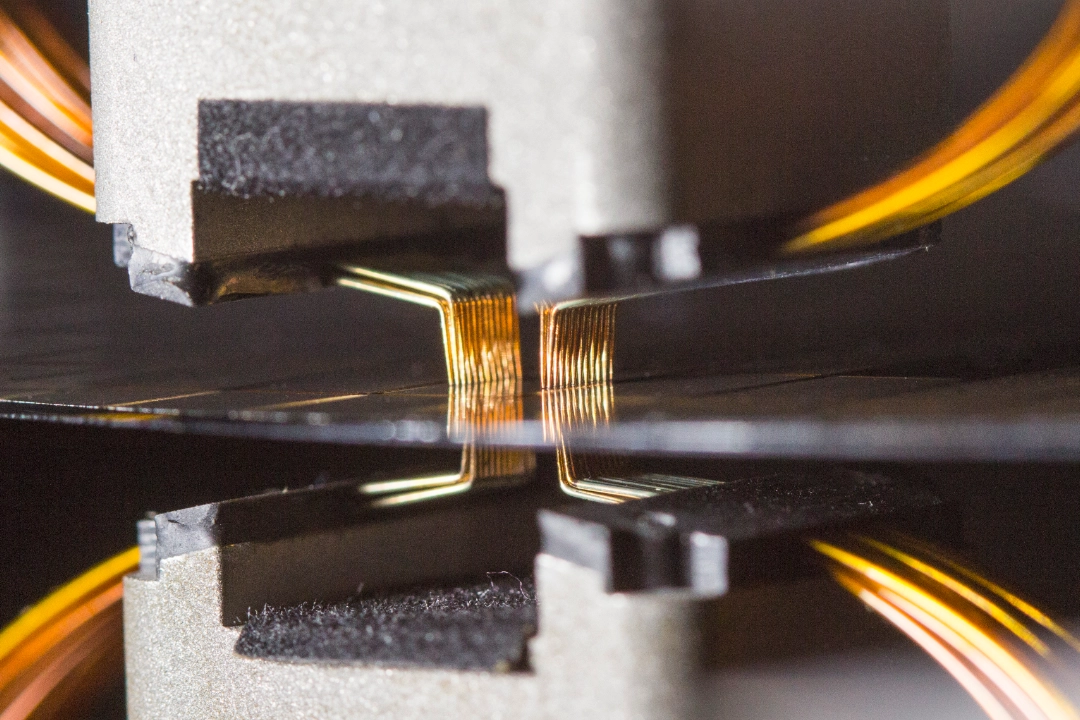
Figure 3 – Simultaneous probing on both sides of a wafer, through flying probe cards on a SPEA TH2000 prober.
5. Future Outlook: The Impact of Layout Optimization on Wafer Testing Evolution
As chip architectures continue to evolve, the semiconductor industry is likely to see an ongoing emphasis on die layout optimization as a means of reducing costs and maximizing yield. The demand for complex wafer designs will continue to rise, driven by applications like IoT devices, AI processors, and miniaturized medical electronics. Each of these areas requires high-density silicon integration, increased functionality, and robust performance—all achievable through innovative die layouts and multi-layer structures.
To keep up with these trends, wafer testing methodologies must evolve accordingly. The adoption of double-sided probers based on flying probe card technology in wafer testing represents an important step forward, providing flexibility, adaptability, and cost efficiency that traditional probe cards cannot offer for many next-generation wafer designs. As probe technology becomes more sophisticated, manufacturers can anticipate further reductions in test time and costs, with improved reliability in assessing even the most intricate wafer configurations.
Conclusion: Meeting Tomorrow’s Semiconductor Challenges with Flexible Testing Solutions
Innovative die layouts are reshaping the approach to wafer design, maximizing silicon efficiency to reduce costs and improve functionality. However, these advancements bring about new challenges in wafer testing, requiring adaptable and versatile probing solutions. Flying probe card technology, with its independent and mobile probe cards, offers a groundbreaking solution to these challenges. By enabling efficient and thorough testing of non-standard dies, MPWs, double-sided wafers, and multi-layer structures, this new generation of wafer probers is becoming indispensable for advanced semiconductor manufacturing. As the semiconductor industry pushes the boundaries of design, flexible and innovative test solutions like double-sided probers based on flying probe card technology will play a critical role in supporting these cutting-edge developments.