Volpiano (Italy)
July 09, 2025
Modern Wafer Testing: How Flying Probe Cards Reduce Costs & Time

The rapid evolution of semiconductor devices toward smaller, more powerful, and multi-functional units has placed unprecedented demands on wafer testing processes.
As advanced architectures and new materials redefine chip layouts and functionality, traditional wafer testing methods struggle to keep up. The development of flying probe card technology introduces a significant shift in wafer probing, offering adaptable and efficient solutions for complex testing requirements while aiming to reduce costs per die.
This article dives deep into the latest trends affecting wafer testing and explores how flying probe technology is revolutionizing this crucial phase in semiconductor manufacturing.
Challenges in Modern Wafer Testing
The primary drivers behind the changes in wafer testing include the rise in demand for high-performance devices and the push toward minimizing physical space while maximizing output. The conventional approach to wafer testing involves placing a wafer on a testing chuck and using a fixed probe card to contact test points across the wafer. This setup works well for uniform chip designs but encounters limitations with non-standard wafer layouts, multiple project wafers, and double-sided dies. Additionally, the industry’s move towards smaller geometries and 3D integration adds layers of complexity, often driving up costs and test time.
Key challenges impacting wafer testing today include:
- Non-standard die geometries: Traditional rectangular dies are giving way to unconventional shapes (e.g., L-shaped, trapezoidal, elongated rectangles) to maximize wafer surface utilization and facilitate more efficient layouts. These novel configurations often result in uneven or mirrored geometries that do not align with standard probe cards, complicating the probing process.
- Multi-project wafers (MPW): Especially common for prototype or small-batch production, MPWs contain diverse chip designs with different configurations and test needs. This layout optimizes costs by merging different designs onto a single wafer but makes uniform testing challenging due to the variance in die size, shape, and pad locations.
- Double-sided and multi-layer dies: With the rise of 3D packaging, dies increasingly contain pads on both sides or feature multi-layer designs for vertical integration. Traditional probe methods, which operate on a single side of the wafer, are often inadequate, requiring multiple wafer insertions or custom equipment.
These complexities not only challenge existing test methods but also drive up test times and costs. The response from the industry has been the development of flying probe technology, designed to offer the adaptability required to handle non-standard wafer layouts and multi-dimensional structures.
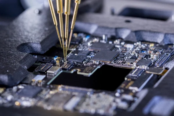
What is Flying Probe Card Technology?
Flying probe card technology represents a shift from stationary probe cards to highly mobile probe units that can independently navigate the wafer surface. Unlike traditional wafer probers, where the wafer moves underneath a fixed probe card, flying probe card systems utilize multiple small probe cards mounted on robotic arms, enabling each probe to maneuver in three dimensions (X, Y, Z) across the wafer’s surface. This flexibility is a direct evolution of how flying probe technology has been used for decades in Printed Circuit Board Assembly (PCBA) testing.
In PCBA testing, flying probes became popular as an alternative to the In-Circuit Test (ICT) bed-of-nails fixtures, which are customized for each specific board layout and can be costly and time-consuming to reconfigure. Flying probes, however, can be programmed to navigate and access different test points without the need for fixed-position nails, providing unparalleled flexibility, especially for low-to-medium volume testing or prototypes where changes in layout are frequent. The technology’s high accuracy and the ability to adjust probe angles and pressures also allow it to perform delicate probing without damaging fine-pitch components or pads, making it particularly useful for high-density assemblies.
This same flexibility is now being leveraged in wafer testing. Flying probe card systems adapt to complex die layouts and unique wafer configurations with ease, making them especially valuable for multi-project wafers, non-standard die geometries, and double-sided designs. By repurposing this proven flexibility from PCBA testing, flying probe technology proves to be a powerful tool for the demands of modern wafer testing, enabling:
- Higher parallelism: Multiple probes can operate simultaneously on different parts of the wafer, significantly improving throughput.
- Enhanced Flexibility: Each probe can independently align to specific dies, making it suitable for complex, non-uniform wafer layouts.
- Double-Sided Testing: With probes on both the top and bottom of the wafer, flying probes can test double-sided dies in a single insertion, as well as enable continuity testing across both sides of pass-through dies.
How Flying Probe Card Technology Enhances Wafer Test Efficiency
Flying probe card technology enables innovative approaches to tackle the complexities of modern wafer testing. Here’s a closer look at the specific features and functions that make this technology transformative:
1. Single-Insertion Testing for Multi-Project Wafers
In traditional testing, each unique die layout within a multi-project wafer would require a separate probe card or multiple prober insertions to fully test the wafer. With flying probe card technology, each probe arm can be assigned to specific dies or test patterns within the wafer. For example, one probe arm might be configured to test an elongated rectangular die, while another could handle L-shaped dies. This reduces the need for swapping probe cards and significantly lowers insertion and alignment times, streamlining the test process.
2. Dual-Side Probing for Double-Sided Wafers
Double-sided wafers, featuring exposed pads on both sides of the silicon, pose significant test challenges. Standard probers require separate insertions for each side of the wafer, necessitating alignment recalibrations. Independent, top-and-bottom flying probe cards solve this, being capable of contacting both sides simultaneously and allowing for:
- Continuity Testing: By testing pad connections on both sides, flying probe card systems enable pass-through die verification and advanced electrical testing.
- Multi-Layer Wafer Testing: Complex devices like MEMS (microelectromechanical systems) often require multi-layer testing for mechanical and electrical functionality. Flying probe cards simplify this process by enabling precise alignment and access to each layer or exposed pad.
3. Optimization for Non-Standard Die Geometries
Many modern wafer designs maximize surface area by using non-traditional die shapes, which can lead to asymmetrical or mirrored layouts on the wafer. Flying probe technology overcomes this by allowing each probe card to be customized for a particular geometry. This flexibility extends testing capabilities to non-standard geometries without the need for additional probe card configurations. For example:
- Customizable Probe Card Layouts: Each probe card can be configured independently, making it easier to test irregular die shapes.
- Mirrored and Rotated Layouts: The probes can independently adjust to the orientation of each die, simplifying the process of testing mirrored or rotated layouts, as seen with some high-density device applications.
4. Automatic Warpage Compensation and Probe Mark Detection
As wafers grow thinner and more complex, warpage—bending due to stress or processing techniques—becomes a more significant issue, impacting probe alignment. Flying probe card systems can incorporate advanced laser-based surface mapping to assess wafer planarity, automatically adjusting each probe’s position to match the wafer’s curvature. This compensation ensures precise contact, minimizing probe-to-pad misalignment and reducing damage risks.
Additionally, probe mark detection is enhanced through high-resolution optical inspection systems. Images captured before and after probing verify contact points, helping engineers to monitor and optimize the accuracy of each probe contact. This combination of laser mapping and optical inspection results in a robust, automated solution for maintaining probe alignment, even on warped wafers.
Applications and Implications of Flying Probe Cards in Wafer Testing
Wafer probers based on flying probe card architecture have applications across various sectors, from consumer electronics to automotive and medical devices. Their ability to handle complex wafer designs, higher-density chips, and unconventional die shapes opens the door for advancements in:
- Miniaturized medical devices: These require multi-functional chips in very compact forms, often using double-sided or multi-layer dies.
- Power electronics: Devices requiring high-current testing, such as power transistors, benefit from flying probes’ precision and versatility.
- MEMS devices: MEMS applications, with their multi-layer structures, also benefit from flying probe card ability to access and test each layer without reconfiguration. High-precision measurement capabilities, such as resistance and capacitance tests, are achievable due to the precise control of probe positioning.
- Automotive and Aerospace Electronics: The automotive industry demands high reliability for sensors and control devices, often produced in low-to-mid volumes with high customization. Flying probe card systems facilitate efficient MPW testing, essential for these smaller production volumes.
- Advanced Consumer Electronics: Miniaturized devices, especially wearable and IoT technology, require dense packing and often involve double-sided or multi-layer designs. Flying probe cards support continuity testing and layer-by-layer testing without compromising speed or accuracy.
Improving Test Cost Efficiency and Time-to-Market with Flying Probe Card Technology
One of the most attractive aspects of flying probe card technology is its ability to reduce test costs and accelerate time-to-market for semiconductor devices. By minimizing the need for multiple insertions and reducing probe card changeovers, flying probe card streamline wafer-level testing. This directly impacts production cycles, making it possible to test more wafers in a shorter timeframe.
Additionally, flying probe card can adapt to new device configurations with minimal adjustments, future-proofing the testing process against further innovations in wafer design. For manufacturers, the impact is twofold: testing processes can keep up with rapid design changes, and costs are managed by limiting the need for custom probe cards and reducing labor-intensive reconfigurations.
Conclusion
Flying probe card technology is transforming the landscape of wafer testing by introducing unprecedented flexibility, precision, and adaptability. As the semiconductor industry continues to innovate with more complex, compact, and multifunctional devices, flying probe card offer a versatile solution capable of meeting the testing demands posed by new chip architectures and non-standard wafer layouts.
For companies developing advanced semiconductor devices, flying probe card technology offers a pathway to optimize test processes, reduce overall costs, and accelerate the journey from wafer to end product. This technology not only addresses immediate testing challenges but also sets the stage for future testing innovations as chip designs evolve.
Flying probe card technology represents more than just a new tool – it marks a paradigm shift in how we approach semiconductor testing, allowing the industry to push the boundaries of what is possible in device design and performance.