Volpiano (Italy)
December 17, 2025
Mastering The 5 Foundational Pillars of Modern PCBA Testing
PCBA testing is non-negotiable for guaranteeing the maximum reliability of modern electronics. However, escalating technological complexities, from extreme density to latent defects, pose severe challenges. Failures to address these with a cutting-edge PCBA tester or Automatic Test Equipment (ATE) can lead to delays, soaring costs, and critical returns from the field. Recognizing these obstacles and adopting advanced testing solutions is essential for maximizing manufacturing efficiency and competitive advantage.
Manufacturers must master 5 critical pillars to ensure excellence in PCBA testing:
- Accessibility in high-density boards
- Test pad integrity
- Latent defect detection
- Modernization investments
- Data management
1. Accessibility in High-Density PCBAs
The relentless push toward miniaturization results in extremely dense PCBAs. Increased interconnectivity and a high population of micro-SMDs drastically reduce available space, often eliminating dedicated test pads entirely. This density poses the primary hurdle for a reliable PCBA test. Traditional In-Circuit Testers (ICT) relying on a fixed PCBA test fixture (bed-of-nails) are structurally inadequate due to these severe accessibility constraints.
Conversely, Flying Probe Testers require no expensive fixtures, providing the flexibility to access all test points with pinpoint accuracy. For manufacturers, this directly leads to improved operational efficiency and a major reduction in Non-Recurring Engineering (NRE) costs. The result is rapid testing for prototypes and production volumes, guaranteed with full fault coverage.
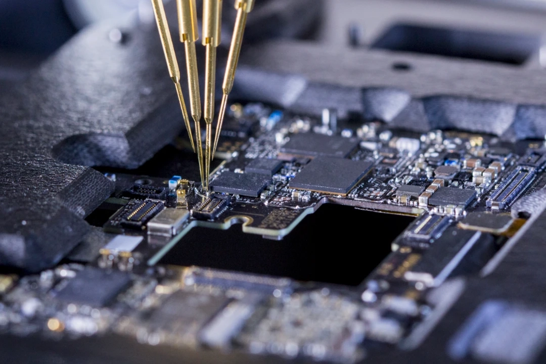
2. Test Pad Integrity
Modern flying probe PCBA tester platforms do more than just ensure physical access; they are the only automatic test equipment capable of contacting small test pads, even on extremely delicate printed circuits.
Establishing contact on fragile substrates requires ultra-precise control over the probe’s landing force, a technical imperative for component integrity. Inadequately modulated contact force can generate false defects and, critically, risks irreversible mechanical damage and latent failure, compromising the final assembly’s reliability.
To address this, the most advanced PCBA testing equipment uses high-speed linear motors that precisely modulate and regulate the probe’s landing force and speed. This “soft touch” technology mitigates impact and prevents marks or abrasions, safeguarding the structural integrity and long-term reliability of the electronic device.
Furthermore, sophisticated algorithms conduct in-depth, predictive testing analysis of the board layout to prevent collisions with taller components, optimizing the test program flow. This synergy of high mechanical precision and software algorithms dramatically reduces the need for retests and debugging.
3. Latent Defect Detection
Insidious faults, such as intermittent connections, signal integrity degradation, and parametric drift often evade standard electrical tests, becoming the primary cause of costly field anomalies and product returns. Adopting an integrated and predictive strategy is an unavoidable technical requirement.
Advanced flying probe systems act as a comprehensive PCBA functional tester, employing a multi-domain approach. They integrate electrical, optical, mechanical, thermal, and functional tests onto a single platform for exhaustive diagnostic coverage. However, the core innovation involves integrating parametric ICT and Artificial Intelligence (AI).
- Parametric ICT targets the core of devices to identify components with compromised integrity or out-of-tolerance drift, necessitating detailed examination or preventive replacement.
- AI, synergizing with advanced optical testing, exponentially boosts diagnostics by leveraging dynamic defect databases. Furthermore, AI enhances operational flexibility by autonomously generating test programs, even when full CAD data is unavailable.
These sophisticated diagnostic capabilities enable manufacturers to certify superior product longevity, transforming fault prevention into a key factor for success.
4. Optimization of Obsolescence and Upgrade Costs
The economic barrier of upgrading or replacing obsolete ICT testers is significant, encompassing not just equipment costs but also integration, training, and program adaptation.
These constraints often slow innovation and erode competitiveness. It is therefore vital to adopt solutions that optimize investment, such as using:
- Universal receivers to integrate existing ICT PCBA test fixtures (bed-of-nails)
- Automatic systems for transferring legacy test programs
This hybrid approach reduces investment costs, facilitates a gradual and sustainable technological transition, and maintains operational efficiency without sacrificing quality, ensuring long-term competitive advantages in PCBA testing.
5. Integrated Data Management
The final critical pillar is managing the fragmented data flow from non-networked test equipment. This lack of real-time comprehensive vision hinders the timely identification of anomalies, defects, and yield loss, severely impacting efficiency. Overcoming this complexity requires:
- Adopting advanced automatic test equipment capable of instant data exchange
- Employing predictive maintenance algorithms
- Ensuring continuous operational monitoring
Intelligent testers anticipate potential downtime and optimize resource management, leading to proactive supervision and systemic improvement of the entire manufacturing process.
Conclusion
The reliability of modern electronics begins and ends with robust PCBA testing. Given the escalating challenges of extreme miniaturization and complex latent defects, advanced strategies are not optional, they are essential.
The pathway to success requires unifying precision PCBA testers with AI synergy, integrated diagnostics, and proactive data management. This unified approach is the decisive factor in optimizing production, ensuring minimal scrap, and securing a clear, competitive edge in time-to-market.