Volpiano (Italy)
March 03, 2026
Combining Boundary Scan & ICT Testing for Assembled PCBs

In an era of rapid PCBA miniaturization and escalating interconnect densities, sustaining a zero-defect production cycle demands the adoption of more sophisticated, integrated testing strategies.
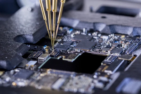
Leveraging circuitry integrated directly within specifically designed components, Boundary Scan Testing (BST) complements the In-Circuit (ICT) and Functional Testing landscape. It provides the necessary capability for detecting open pins and short circuits on complex microprocessor-based boards, specifically targeting hidden nets, often beneath BGA and LGA components, where physical access is impossible.
1. How Does Boundary Scan Testing Work for PCBA
Utilizing a chain of Boundary Scan Cells linked through Test Access Ports (TAP), this test method creates a “virtual bridge” across the PCBA. Programmatically controlled, the system injects digital stimuli through the circuit paths to verify signal integrity.
Boundary Scan test methodology is governed by the IEEE 1149 standard. This standard dictates a specific circuit design and test access mechanism implemented within the integrated circuit (IC) itself, allowing to test the chip’s input/output pins via standardized TDI/TDO (Test Data In/Out) digital ports.
2. Where Does Standalone Boundary Scan Reach Its Limit
Despite its ability, Boundary Scan Testing is not intended to be a complete, standalone testing solution to assure PCBA high-quality production.
While some PCBA manufacturers adopt a test strategy combining Functional Testing with Boundary Scan, this approach leaves a significant void in the PCBA test coverage causing many manufacturing defects to escape detection.
Understanding the specific focus areas of Boundary Scan Testing allows for the identification of critical gaps that must be bridged by additional testing methods:
- Digital Specialization. Typical tests executed during a Boundary Scan Test are interconnect tests, infrastructure tests and in-system programming. It cannot properly test passive devices (resistors, capacitors,…) or active devices (transistors, relays,…). Being fundamentally a digital connectivity test, it cannot measure critical analog values, verify power integrity, or fully test complex RF circuits without supplementary hardware.
- Standard Specific. Boundary Scan Testing can only test the interconnections between components that adhere to the IEEE 1149.1 standard.
- Design First Architecture. The architecture made of controller pins, and specific chaining logic must be intentionally included in the initial PCB design phase.
The most effective way to address these focus areas is through a multi-domain test strategy that incorporates In-Circuit Testing.
3. Why is Combining Boundary Scan with In-Circuit Testing Essential
Integrating Boundary Scan into a conventional In-Circuit Test (ICT) platform, such as a SPEA flying probe tester or bed-of-nails tester, represents the smartest strategy for modern electronics manufacturing to detect faults, internal or external the PCBA, and achieve the highest possible test coverage.
This approach transforms the automatic test equipment into a unified diagnostic engine where the ICT testers handle traditional measurements via analog channels, while seamlessly delegating digital operations to an embedded BST controller. By treating Boundary Scan as another intelligent instrument within the same station, manufacturers eliminate the high operating costs of using two separate test stages.
The synergy between these two techniques provides several critical advantages:
- Process Optimization. Consolidating testing into a single station minimizes manual handling and operator overhead, streamlining the production workflow.
- 100% Fault Coverage. While Boundary Scan Testing tackles inaccessible nets, ICT checks the remaining passive and active components, as well the non-IEEE 1149.1 standard compliant components, ensuring complete detection across the entire PCBA.
- Test Optimization. Advanced operating systems, such as SPEA’s Leonardo OS, automatically select the best technique for each net, eliminating redundancies to significantly reduce overall test time.
- Unified Reporting. Results from both methods are integrated into a single, comprehensive report within the Leonardo OS, making fault detection faster and more intuitive for operators.
- Enhanced Accessibility for Hidden Defects. The combination of Boundary Scan and multi-domain test platforms provides a powerful solution for maximizing fault detection. The result is a dramatic increase in testability for complex PCB architectures, successfully capturing defects in areas once deemed unreachable.
By consolidating fragmented test stages into a single, high-efficiency test platform, the integration of Boundary Scan within In-Circuit Testers significantly reduces operational costs while maximizing throughput. Ultimately, this synergy cements the multi-domain approach as the most powerful solution for achieving exhaustive fault coverage and precision diagnostics in modern electronics manufacturing.